


“Moiré structures can be formed as a result of interference, i.e. the overlapping of two layers of systems with a specific arrangement of points, lines or more complex systems – e.g. atoms in a crystal – rotated by a certain angle,” Professor Maciej Molas, from the UW’s Faculty of Physics says. The recent findings on moiré structures were published in the Science paper co-authored by Prof. Molas.
The newly published review article in Science “Moiré photonics and optoelectronics” aimed to collect and describe the latest findings in the emerging field of photonics and optoelectronics related to moiré systems, formed by van der Waals layer materials (vdW).
“Moiré structures can be formed as a result of interference, i.e. the overlapping of two layers of systems with a specific arrangement of points, lines or more complex systems – e.g. atoms in a crystal – rotated by a certain angle,” Prof. Molas explains. The perfect candidates for studying such effects are vdW materials because of the weak interactions between the subsequent layers. This makes it possible to abrade them to single atom-thin monolayers, e.g. a single layer can be obtained from a volumetric graphite – graphene,” Prof. Maciej Molas from the Faculty of Physics, University of Warsaw, explains.
The article co-authored by Prof. Molas also discusses future possible research directions in this field. They could lead to potential technological innovations in nanotechnology, such as light-emitting diodes with previously unknown optical and electronic characteristics and properties.
“In 2010 Prof. Andre Geim and Prof. Kostya Novoselov received the Nobel Prize in Physics for the groundbreaking experiments regarding the two-dimensional graphene. Since then, the scientists’ interest in van der Waals (vdW) materials has expanded rapidly. This applies primarily to the area of semiconductor physics and nanoscience as well as optoelectronic applications,” Prof. Molas adds.
Atomically thin layers of vdW materials represent a new class of substances, with properties that differ significantly compared to those of their bulk counterparts. Although over 2000 vdW materials have been discovered so far, grouped into several dozen families, including semiconducting transition metal dichalcogenides (e.g. molybdenum disulphide) or magnetic chromium trihalides (e.g. chromium triiodide), scientists also undertake the fabrication of new structures by combining materials with different properties.
“However, unlike the classic three-dimensional materials used today in electronics and optoelectronics, such as silicon or gallium nitride, the distances between atoms do not play a role in the assembly of such artificial structures as a result of the weak vdW interactions between subsequent layers. A parameter that has a significant impact on the properties of such structures is the twist angle between adjacent layers. Choosing the right twist angle between two layers of vdW materials can lead to the appearance of the so-called moiré pattern,” the UW researcher says.
The figure demonstrates the top view of two twisted monolayers (MLs), i.e., the molybdenum diselenide ML on top of the tungsten diselenide ML with a relative rotation angle of 5 degree. A new pattern can be seen in the figure, which is known as a moiré superlattice. The distances between the characteristic elements in the moiré superlattice are significantly greater than the distances between the atoms in individual MLs.
“This leads to the observation of not only a new crystal structure, but mainly contributes to the emergence of innovative electronic and optical properties in the moiré structure, which stimulates the exploration of completely new physics and devices with novel architecture,” Prof. Molas concludes.
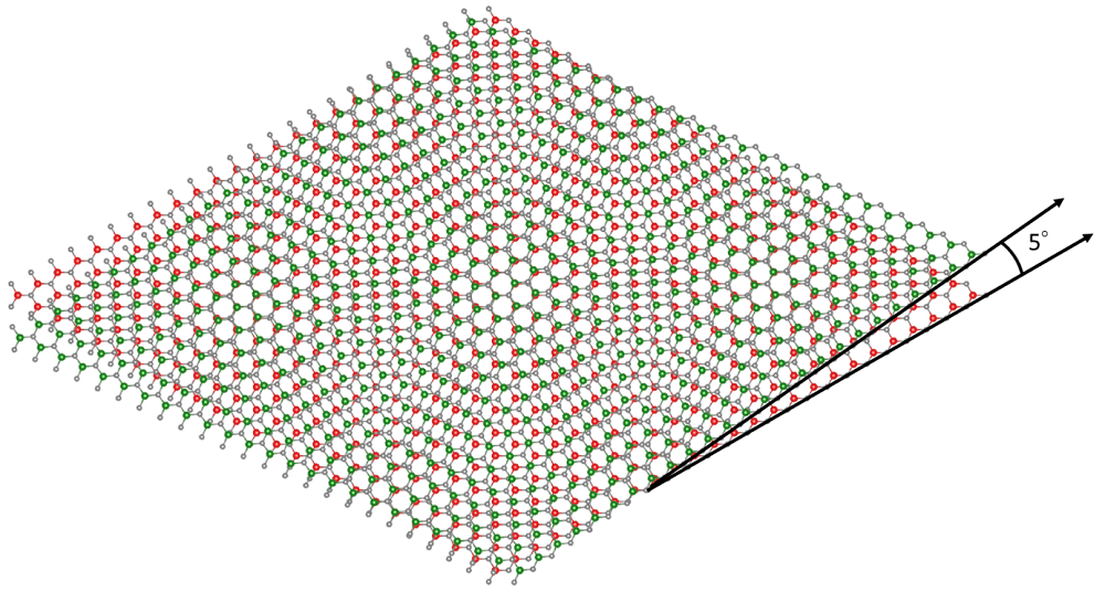
Schematic representation of the moiré superlattice observed in the twisted two monolayers of molybdenum (Mo) and tungsten (W) diselenides with a relative angle of 5 degrees. The green and red balls represent correspondingly the Mo and W atoms, while the grey balls denote the selenium (Se) atoms. Credit: Maciej Molas.